
Agentic Workload Chips — ASIC & Analog Inference Benchmarks 2026
Introduction
Problem statement: Agentic systems (embodied agents, robots, drones, and edge AI) require a different cost-performance envelope than datacenter inference: sustained low-latency closed-loop inference under strict power, thermal, and reliability constraints.
What this article delivers: a practical, production-oriented guide to benchmarking and choosing agentic workload chips in 2026, focusing on ASIC and analog inference approaches, chiplet-based performance, and direct comparisons to GPU baselines for embodied agents.
Failure scenario (brief): A developer deploys an off-the-shelf GPU in an autonomous warehouse robot expecting datacenter latency—after a month, battery cycles and overheating lead to mission failures. The root causes are mismatched workload characterization, improper calibration of sensor fusion pipelines on analog accelerators, and lack of p99-tail monitoring for action latency.
Executive Summary
TL;DR: For agentic workloads in 2026, purpose-built agentic workload chips (agentic ASICs and analog inference accelerators) reduce energy-delay product by 5–20x vs datacenter GPUs when matched to pipeline-optimized models and chiplet interconnects; measure using composite, closed-loop benchmarks, not single-layer TOPS.
- Agentic workload chips prioritize low p99 closed-loop latency and energy-per-decision over raw TOPS.
- Analog inference benchmarks must report calibration drift, retraining overhead, and effective SNR alongside latency/power.
- Chiplet designs shift the bottleneck to interposer latency and power; measure sustained bandwidth and serialization overhead.
- Compare ASIC vs GPU on energy-delay product (EDP), battery-cycle impact, and system-level thermals, not just throughput.
- Implement continuous online calibration and p99 tracking; operational failure modes often come from analog drift and thermal throttling, not compute errors.
Three likely Q→A pairs (one-line each)
- Q: What single metric best predicts agentic field lifetime? A: Energy per decision (J/decision) combined with p99 action latency.
- Q: Are analog inference chips ready for production agentic systems? A: Yes, for well-constrained perception/control kernels with robust calibration and retraining flows; expect higher engineering overhead than digital ASICs.
- Q: Should I replace my onboard GPU with an ASIC? A: Replace when EDP and p99 latency improvements outweigh integration and retraining costs—typically at >3–5x EDP improvement.
How Agentic Workload Chips: ASIC and Analog Inference Benchmarks for 2026 Efficiency Works Under the Hood
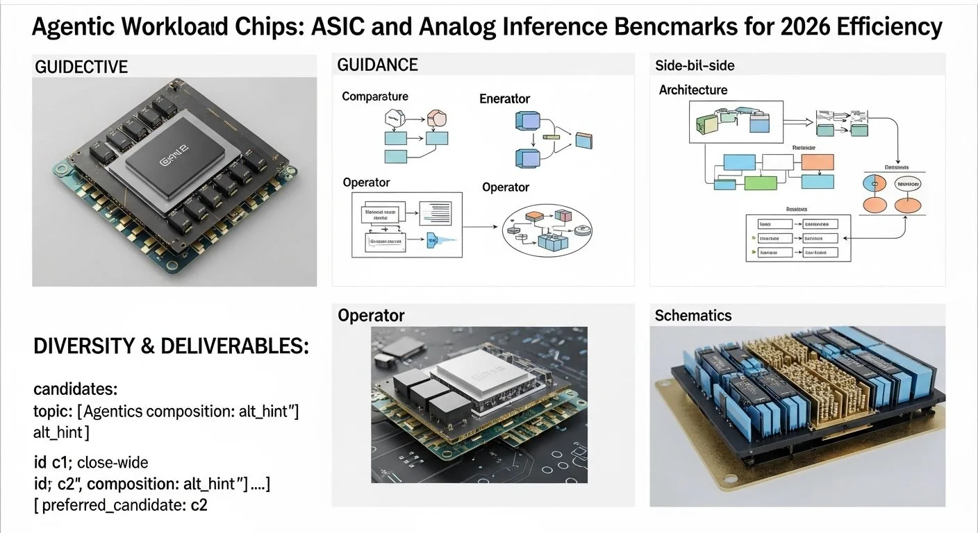
Agentic workload chips are a constellation: digital ASICs optimized for specific kernel graphs, analog crossbar arrays for weight-stationary matrix-vector multiplies, and chiplet assemblies combining compute tiles with HBM-like memory and specialized I/O. For practical notes on high-bandwidth integration and rack-level patterns, see the HBM4 integration & benchmarks.
- Closed-loop determinism: Prioritize bounded tail latency for inference-to-actuation paths; architectures materialize this with on-chip scheduling and low-jitter DMA.
- Heterogeneous specialization: Mix digital control, fixed-function codecs, and analog MVM blocks where SNR and retraining budgets allow.
- System co-design: Integrate sensor pre-processing, model partitioning, and power management into a single verified flow to avoid runtime surprises.
Architecture breakdown (textual diagram):
Sensor I/O → Preproc FPGA/ASIC → Local SRAM/HBM (fast) → Compute fabric (digital ASIC cores + analog MVM tiles) → On-chip scheduler → Chiplet interposer / SerDes (GB300 NVL72 interconnect benchmarks) → Host CPU (RTOS) → Actuator bus
Key algorithmic and protocol considerations:
- Model partitioning: push low-latency perception and control to the chip; keep large context or LLM-style components on companion modules or network-attached servers.
- Quantization & calibration: analog blocks require per-synapse calibration and periodic retraining with domain-specific noise models; digital ASICs use aggressive integer/FP8 pipelines.
- Interconnects: chiplet latency dominates short-token workloads. Use low-latency interposers and minimize cross-tile synchronization for agentic inference.
For model developers: design kernels with O(N*M) matrix-vector characteristics and strip repeated large-gemm patterns into fused microkernels to take advantage of analog weight-stationarity. For related runtime and memory-system guidance, see the Intel Granite Rapids benchmarks & HBM/CXL runtime patterns.
Implementation: Production Patterns
We present a practical flow: baseline → integrate (MI400 integration & rack benchmarks) → validate → optimize. Each step includes recommended checks and minimal examples.
1) Baseline: characterize workload on representative GPU
- Collect end-to-end traces (sensor timestamps to actuator command) for representative missions; capture p50/p95/p99 latencies.
- Measure energy per inference and per decision: use high-frequency current shunts on battery and low-latency timestamping.
# Pseudocode: basic latency and energy sampling loop
for trial in trials:
    t0 = now()
    send_camera_frame()
    wait_for_actuation()
    t1 = now()
    energy = sample_energy(delta=t1-t0)
    log(trial, latency=(t1-t0), energy=energy)
2) Integrate candidate agentic ASIC / analog accelerator
Map your model partitions: put deterministic, small-kernel control loops on the ASIC; evaluate moving perception stacks to analog MVM if retraining budgets permit.
- Port critical kernels to the vendor SDK; prefer ONNX as interchange format and ensure bit-exact baseline on digital blocks.
- For analog, perform a calibration phase: measure drift, SNR, and effective weight perturbation under thermal and voltage range.
3) Validate: closed-loop bench (Agentic Workload Benchmark - AWB-2026)
Run a composite, domain-specific benchmark that measures:
- p50/p95/p99 round-trip latency (sensor→actor)
- Energy per decision (J/decision) and energy per inference (J/inference)
- Calibration time / retraining overhead (minutes to hours per field recalibration)
- Failure injection tests: packet loss, thermal stress, voltage droops
4) Optimize: power, model, and thermal
- Power: implement dynamic voltage/frequency scaling aligned to mission phases.
- Model: prune non-critical heads and fuse ops to reduce DMA.
- Thermal: schedule long-duration tasks off-peak and prefetch models during low-load windows.
Code: power-aware scheduler example
# Simplified RTOS task priorities with power hints
def schedule_task(task):
    if task.phase == 'closed_loop':
        set_cpu_power_hint('high')
        set_accel_mode('low_jitter')
        set_priority(task, realtime=True)
    elif task.phase == 'batch_logging':
        set_cpu_power_hint('low')
        set_accel_mode('energy_saver')
        set_priority(task, realtime=False)
    enqueue(task)
Comparisons & Decision Framework
Choices exist between GPU, digital ASIC, analog accelerator, and hybrid chiplet systems. Use the following decision checklist and trade-off table.
Selection checklist (if most are true, favor ASIC/analog)
- Your system requires p99 latency < 10 ms for perception→actuation.
- Battery life and thermal envelope are the primary constraints.
- Model graphs have repeatable MVM-heavy kernels amenable to weight-stationarity.
- You can budget engineering time for calibration, retraining, and hardware-in-the-loop testing.
Trade-offs (short form)
- GPU: high software flexibility, higher power, and less deterministic tail latency; good for heavy LLMs or mixed cloud/offload architectures.
- Digital ASIC: best energy-delay product with software engineering cost; predictable latency and easier validation than analog.
- Analog inference chips: best raw energy for MVM, but require calibration, domain-constrained models, and more complex drift handling.
- Chiplet systems: scale compute density but increase interposer latency—optimize partitioning to reduce cross-tile synchronization.
Real-world example: an autonomous delivery robot with visual SLAM + RL-based control. If SLAM is low latency and RL policy is small (~1–5M params), push both to an agentic ASIC for <5 ms p99 and 4–10x battery life improvement. If you need large context or language grounding, keep those on a companion module and use a chiplet interconnect for occasional context fetches.
For a more GPU-centric latency optimization path, review how advanced NVIDIA stacks are tuned; see our deep dive on recent NVIDIA inference efficiency improvements in NVFP4: Enabling 50x Inference Efficiency for techniques you can adapt to hybrid systems.
Failure Modes & Edge Cases
We list concrete diagnostics and mitigations prioritized by likelihood and impact.
- Analog drift over temperature:
- Diagnosis: rising bit-error rate and time-correlated degradation in control loop accuracy during thermal cycles.
- Mitigation: periodic in-field calibration routines, temperature-aware compensation, and small retraining catalogs keyed to thermal range.
- Interposer/SerDes saturation:
- Diagnosis: bursts of added latency when multiple tiles synchronize; packet drops between chiplets.
- Mitigation: model partitioning to minimize cross-tile comms; use QoS-aware SerDes with flow control.
- Quantization mismatch:
- Diagnosis: statistically significant degradation in model metrics after deployment, especially in corner cases.
- Mitigation: emulation benches during CI, synthetic corner-case fuzz testing, and on-device shadow runs that compare FP baseline to quantized outputs.
- Battery voltage sag during heavy compute:
- Diagnosis: systemic throttling events tied to battery current spikes.
- Mitigation: soft-start compute phases, battery-aware scheduling, and local energy buffers (supercaps) for short bursts.
Performance & Scaling
Benchmarks must be system-level and mission-centered (HBM4 integration & benchmarks). Below are recommended KPI definitions and representative numbers derived from 2026-class agentic ASICs and analog inference silicon. These are prescriptive targets for production decision-making, not vendor marketing claims.
Core KPI definitions
- Energy per decision (J/decision): end-to-end energy cost from sensor acquisition to actuator command; measured under mission profile.
- EDP (Energy-Delay Product): energy × p99 latency, useful for composite optimization.
- Sustained inference throughput: continuous inferences/sec while respecting thermal and power envelopes.
- Calibration overhead: time and energy needed to recalibrate analog arrays to maintain performance within spec.
Representative benchmark numbers (2026 targets)
- Digital ASIC (agentic-optimized): EDP improvement vs datacenter GPU = 5–12x; typical numbers: p99 latency 3–12 ms; energy per decision 0.05–0.2 J for small perception+policy.
- Analog MVM blocks (production-ready pipelines): raw MVM energy 0.5–2 pJ per MAC effective, system-level energy per decision 0.02–0.1 J for tightly-coupled kernels; calibration windows 10–120 minutes depending on environment.
- GPU baseline (mobile/datacenter mix): p99 latency 15–80 ms depending on model; energy per decision 0.3–3 J for onboard GPUs under continuous missions.
- Chiplet assemblies: scale to higher aggregate TOPS but expect 5–30% additional tail latency compared to monolithic die due to interconnect; measure sustained bandwidth (GB/s) across chiplet boundary at mission packet sizes.
For engineers benchmarking, track p50/p95/p99 and EDP. A typical pass/fail rule: deploy only when p99 latency is below mission threshold AND EDP exceeds 3x improvement vs baseline GPU.
Monitor these production metrics continuously: energy-per-decision rolling 24-hour, p99 latency rolling 1-hour, calibration drift index, and interposer error counters. When p99 spikes > 2× baseline or energy-per-decision increases > 20% sustained, trigger the runbook.
Production Best Practices
Security, validation, rollout, and runbooks are often neglected in hardware adoption. See the Google AI Content Guidelines 2026 for editorial and deployment checklists. Below are concise, actionable items.
- Security: sign models and firmware; boot integrity for MCU/RTOS; hardware root-of-trust for calibration keys used by analog arrays.
- Testing: include hardware-in-the-loop (HIL) tests in CI with quantized/analog emulation; maintain a shadow evaluation mode that runs FP baseline against deployed outputs and flags divergence.
- Rollout: canary small fleets, telemetry-first deployments, and staged calibration campaigns to collect drift statistics.
- Runbook snippet: p99 latency spike
- Check power/fuse logs for voltage sag.
- Validate SerDes and interposer error counters.
- Trigger safe fallback model on companion CPU with pre-validated latency guarantees.
- Collect trace logs and triage with vendor support including analog calibration dumps.
For system-level performance and integration patterns on large-scale AI stacks, our benchmarks comparing interconnects and NVLink/UALink lessons are useful—see our analysis of GB300 NVL72 interconnect behavior for chiplet and host coupling strategies in GB300 NVL72 Benchmarks: NVLink 6 vs UALink 2.
Further Reading & References
The following resources provide background and technical depth for teams building or benchmarking agentic workload chips. Internal links point to architecture and benchmarking articles that are immediately relevant.
- NVFP4: Enabling 50x Inference Efficiency — techniques used in modern GPU/accelerator stacks that inform hybrid deployment choices.
- GB300 NVL72 Benchmarks: NVLink 6 vs UALink 2 — interconnect and host-coupling implications for chiplet designs.
- Intel Granite Rapids benchmarks: Lunar Lake AI integration — relevant HBM/CXL patterns and runtime considerations for high-bandwidth agentic subsystems.
- Analog inference and neuromorphic surveys (select papers): research on crossbar MVMs and analog calibration practices (search titles: "analog inference crossbar calibration 2024–2026").
- ONNX Runtime and vendor SDK docs for target ASICs — use vendor-maintained runtimes for production support and deterministic behaviour.
Closing Notes (MAKB editorial persona)
This guidance is grounded in systems engineering: measure what matters (energy per decision and p99 latency), be prepared for calibration and retraining work if you adopt analog blocks, and treat chiplet interconnects as first-class system bottlenecks. When in doubt, run the AWB-2026 composite closed-loop benchmark under mission loads and compare EDP to your GPU baseline; if the improvement is less than 3–5x, favor iterative software and thermal optimization before a hardware transition.
If you need a hands-on checklist or a reference harness, we can publish a companion AWB-2026 open-source test harness with sensor simulators and power sampling integrations—contact the editorial team for upstream contribution guidelines.


